InnovotypeElectronics design studio
Portfolio

Hardware designed for where it gets deployed.

Each project is written up as problem, approach and outcome, with the key specifications alongside.

Entry 01 / 06 · Flagship · In progressLoRaWAN · Solar · Multi-sensor
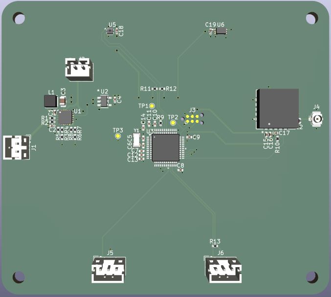
Soil sensor node PCB, top view
Soil sensor node, top viewFig. 01
100 nodes · 5-year TCOUSD
Commercial tier~50,000
Innovotype node (target)< 15,000

Multi-sensor Soil/Environmental LoRaWAN Node

MCUSTM32L431
RadioSX1262 (E22-900MM22S)
PowerSolar + LiFePO4
SensorsSoil moisture · soil temp · air T/RH
Problem
Agricultural and environmental sensing deployed by the hundred is priced out of reach. A 100-node commercial deployment runs to roughly USD 50,000 over five years, while hobby-grade boards don’t survive in the field.
Approach
Reliability-grade engineering at hobby-tier deployment economics — GCC/Saudi-first, with UK and Australia planned for v2. A long-range LoRa link (SX1262, via a U.FL-to-bulkhead antenna) runs from a low-power STM32L431. Power is solar-harvested through a BQ25570 into a LiFePO4 buffer on a single regulated rail, so the node runs maintenance-free in the field. Sensing covers soil moisture, soil temperature and air temperature/humidity, housed in a field-serviceable enclosure.
Outcome
Board design complete — 86 × 77 mm layout routed and ready for fabrication. Target: a sub-USD-15,000 five-year total cost of ownership for a 100-node deployment.
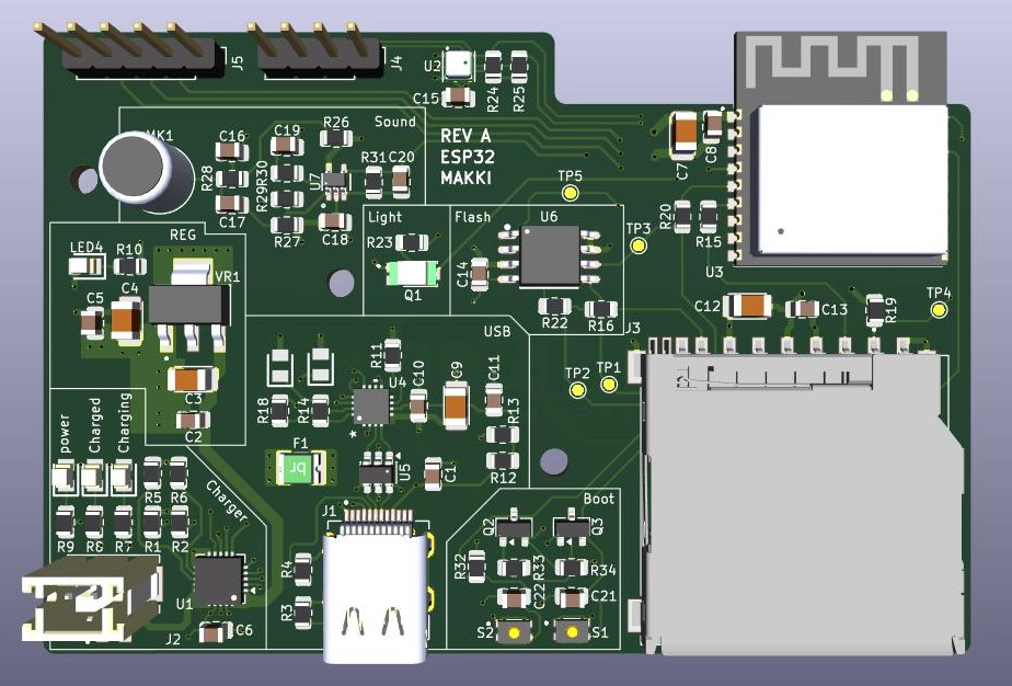
Entry 02 / 064-layer · ESP32-C3 · Wi-Fi/BLE
ESP32-C3 IoT development board, 3D render
ESP32-C3 four-layer development board, top viewFig. 02

ESP32-C3 IoT Development Board

Layers4
MCUESP32-C3
PowerUSB-C + BMS
StoragemicroSD + flash
Problem
IoT prototypes need a single board that covers wireless connectivity, sensing, storage and battery operation.
Approach
A 4-layer board built around the ESP32-C3 wireless SoC with:
  • power management and a battery management IC
  • USB-C power and data via a USB–UART bridge
  • SD card and on-board flash
  • environment and ambient light sensors, plus a microphone
  • boot and reset buttons
Outcome
A complete IoT development platform with on-board sensing, storage and a full USB-C power/data path.
Entry 03 / 062-layer · TI MSPM0 · MEMS
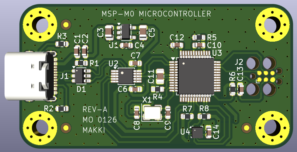
MSPM0 accelerometer board, 3D render
MSPM0 two-layer accelerometer board, top viewFig. 03

MSPM0 Accelerometer Board

Layers2
MCUTI MSPM0
Sensor3-axis MEMS
DebugSWD
Problem
Step counting needs a low-cost motion-sensing board that is easy to program and robust to handling.
Approach
A 2-layer TI MSPM0 board with a triple-axis MEMS accelerometer, external crystal oscillator, USB-C with UART bridge, ESD protection on exposed I/O, and an SWD programming port.
Outcome
A compact, low-cost MEMS step-counter board with full debug access.
Entry 04 / 064-layer · SSOP-20 · Orientation
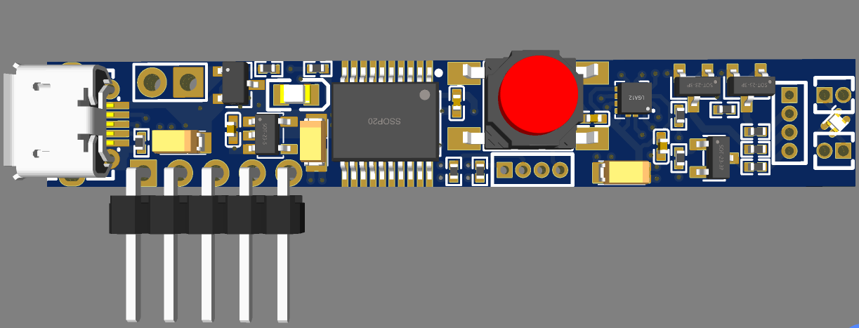
Tiny RGB LED PCB, 3D render
Tiny SSOP-20 four-layer RGB LED boardFig. 04

Tiny RGB LED PCB

Layers4
MCUSSOP-20
SensorAccelerometer
PowerUSB-C + battery
Problem
Packing a microcontroller, motion sensing, battery charging and an LED output into a palm-sized board.
Approach
A 4-layer board with an SSOP-20 microcontroller, accelerometer, RGB LED, push button, battery connector and USB-C charge path.
Outcome
The RGB LED changes colour with the board’s orientation, on a palm-sized 4-layer layout.
Entry 05 / 064-layer · STM32H573 · 35×35 mm
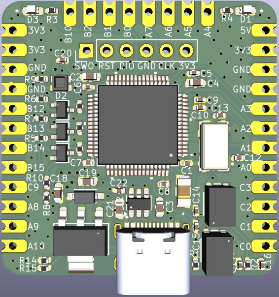
Custom STM32H573 development board, top view
Custom STM32H573 board, top viewFig. 05

Custom STM32H573 Dev Board

Layers4
MCUSTM32H573
Size35 × 35 mm
DebugSWD
Problem
High-performance MCU prototyping needs a compact board with clean power, accurate timing and full debug access.
Approach
Built from scratch around the STM32H573RIT6 (250 MHz, 2 MB flash):
  • 8 MHz HSE crystal + 32.768 kHz LSE for the RTC
  • 5 V→3.3 V LDO with USB-C power and data
  • USBLC6 ESD clamp on USB D+/D−
  • SWD header (SWCLK/SWDIO/SWO/NRST) with BOOT0 and NRST buttons
Outcome
A 35 × 35 mm board, USB-C powered and programmed, with GPIO broken out for prototyping.
Entry 06 / 06IPC-compliant · DFM/DFT
ABSTRACT VISUAL ONLY — NO IDENTIFYING DETAIL
High-reliability robotic hardware for mission-critical environmentsFig. 06

High-reliability robotic hardware

DomainRemote handling
StandardIPC
FocusDFM / DFT
Duration4 years
Problem
Remote-handling robotic systems in mission-critical environments need PCBs that work first time and keep working.
Approach
Schematic and PCB layout to IPC standards, with DFM reviews, DFT requirements built into design verification, and direct fabricator liaison on stack-up, technical queries and quality.
Outcome
Manufacturable boards delivered through the full PCB lifecycle. An equipment database cut BOM preparation time by 40%.
Next step

Start with a design audit.

A call to review your requirements, constraints and timeline, and agree which engagement fits.