Electronics design for IoT and connected hardware. From sensors to industrial controllers — concept to certified hardware, fast.
For funded IoT and connected-hardware teams across the GCC, UK, and Australia/NZ.
Four ways to engage
Starting-from ranges in USD. Final scope is set after the design audit.
Design Sprint
Schematic + PCB layout (≤4 layer), BOM, JLCPCB handoff, 1 design review
Prototype Package
Sprint + 5–10 assembled units + firmware bring-up + test report
Productization Sprint
Prototype + DFM + enclosure coordination + small-batch run (50–500 units) + compliance
Fractional EE Retainer
Async + 4–6 hrs sync/week
Senior-level hardware, on a sprint timeline
High-reliability background
Four years designing high-reliability robotic hardware for mission-critical environments.
AI-augmented KiCAD
AI-assisted schematic, review and documentation steps compress timelines without skipping checks.
DFM / DFT expertise
Boards designed to be built, tested and inspected, with IPC-compliant layout and test access from the start.
JLCPCB-ready
Gerbers, BOM and placement files prepared for direct JLCPCB fabrication and assembly.
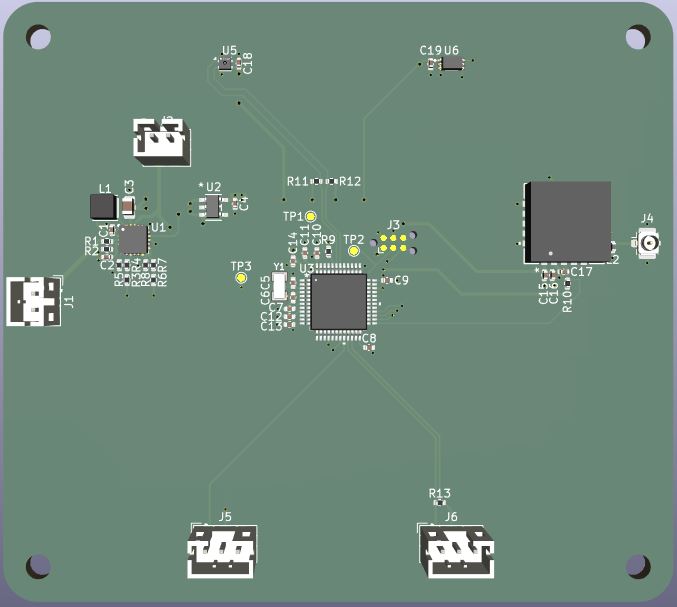
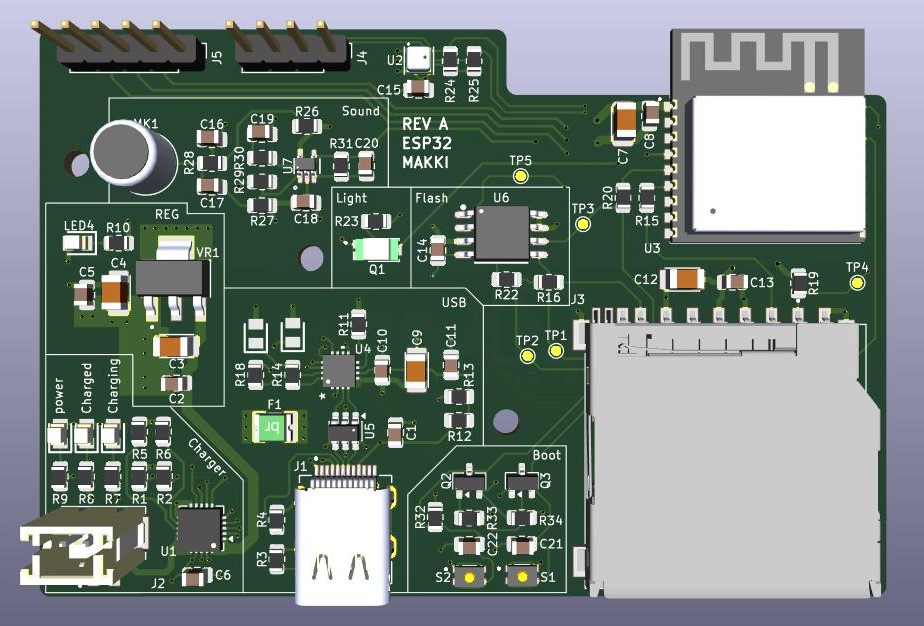
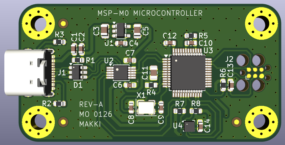
Recent boards
Start with a design audit.
A call to review your requirements, constraints and timeline, and agree which engagement fits.